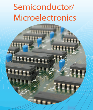
Semiconductors & Microelectronics
From
Wafer Inspection to Integrated Circuit Testing and Failure Analysis to
Micro-processing, Calmar Lasers are enabling the Semiconductor and Microelectronics
World
Today’s consumer electronics industry
has come to rely heavily on lasers as versatile and precise tools in the
manufacturing process. From the
semiconductor chips to printed circuit boards to flat panel displays, lasers support
the entire fabrication chain to enable smaller feature sizes, improved device
performance, increased yields, reduced manufacturing costs and more. Whether it is metrology, lithography,
annealing, micro-drilling, die singulation, patterning, cutting, failure
analysis, etc., unique laser sources ensure an optimum outcome and excellent process
control.
With
their precise material removal and limited peripheral damage, ultrafast (picosecond
and femtosecond) lasers are often the preferred sources for some of these advanced
micromachining applications. Generally,
such lasers operate in the kHz to MHz repetition rate with pulse energies in
the µJ to mJ range and utilize some type of chirped-pulse
amplifier scheme but all require a highly stable, robust seed laser
source. And that’s
Calmar’s expertise. Mendocino OEM laser modules can be found at the heart of many of
these amplified systems. They
are the reliable “black-box” devices that offer seamless integration with the
ability to be customized according to the requirements of the downstream
amplifier.
In the semiconductor wafer inspection
and thin-film metrology areas, ultrafast lasers have also found broad utility. For example, with its compact form factor and
exceptional stability, the Carmel X-series offers the ideal source for second
harmonic imaging and the non-destructive detection of subsurface impurities in
silicon-on-insulator wafers. Similarly, both
the Mendocino and
Carmel X-series are perfect sources for picosecond
ultrasonic measurements of single and multi-layer metal thin films in a variety
of semiconductor devices.
Cazadero and Carmel
X are
also used to enable highly spatialized probing of integrated circuits through two-photon
excitation.
The two-photon absorption-transient current technique (TPA-TCT) is a
powerful inspection tool for high-resolution 3D mapping of the charge
collection junction in semiconductor detectors, while two-photon laser-assisted
device alteration enables the localization of failure sites in integrated
circuits to a precision of ~ 100 nm.
Whether it be a robust, low power,
seed laser source such as the Mendocino or a higher power laser, such as the Carmel or Cazadero, Calmar offers an ultrafast fiber
laser solution for your semiconductor/microelectronics applications.
Mendocino
OEM Ultrafast Laser Modules for Industrial Applications